Samsung's semiconductor division ties up with IISc for R&D on safeguarding computing chips

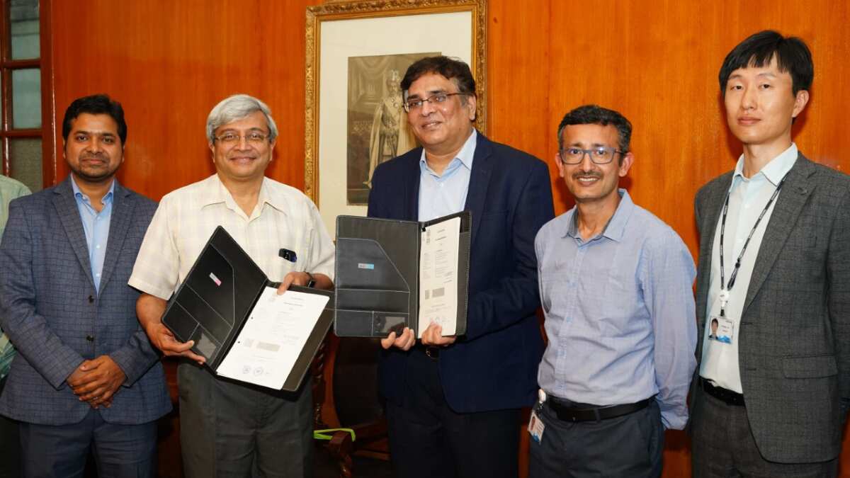
IISc & Samsung tie up for R&D on computer chips
Electrostatic Discharge (ESD) has been a major cause for concern in the computing chip industry, as it causes unexpected destruction of semiconductor devices. The ESD phenomenon is a high-current and short-duration event caused by the transfer of electrostatic charge between two surfaces or bodies. It can happen due to human handling of chips and even robotic handling of chips. It is to develop ESD protection that South Korean Electronics giant Samsung's semiconductor arm and the Indian Institute of Science have joined hands.
The partnership seeks to build cutting-edge ESD device solutions to protect ultra-high-speed serial interfaces in advanced Integrated Circuits (ICs) and system-on-chip (SoC) products. An integrated circuit refers to a circuit compressed into a small-sized chip, whereas a system-on-chip has computer-like capabilities and can run an operating system.The related research will be carried out by ProfessorMayank Shrivastava’s group at the Department of Electronic Systems Engineering (DESE), IISc. Solutions arising from this research will be deployed in Samsung’s advanced process nodes, said the company.

The research agreement was exchanged by Balajee Sowrirajan, CVP & MD at Samsung Semiconductor India Research, Bengaluru, and Prof Govindan Rangarajan, Director, Indian Institute of Science (IISc), in the presence of delegates from Samsung and IISc. "Our goal is also to increase capacity building through training programmes at the postgraduate level, opening up opportunities for students to pursue industry internships, and encourage entrepreneurial ventures by young researchers,"said Balajee Sowrirajan, CVP & MD, SSIR.
ICs and SoCs are essential for any electronic system, large or small. However,they are very susceptible to ESD failures, especially those developed using advanced nanoscale CMOS (Complementary Metal Oxide Semiconductor) technologies. The majority of IC chip failures and field returns are attributed to ESD failures. This is also rare expertise and industries holding the art of designing ESD protection devices and interface concepts lead the market. Thus, R&D in ESD technology for highly reliable interfaces and SoCs that operate at low power and high speed is an integral part of the semiconductor innovation effort. IISc is one of the few institutes in the world leading ESD device research.
&imwidth=180&imheight=135&format=webp&quality=medium)
Brendan Taylor overtakes Andy Flower to become Zimbabwe’s leading ODI run-scorer
&imwidth=180&imheight=135&format=webp&quality=medium)
No Kings' Instagram suspended during early-voting campaign
&imwidth=180&imheight=135&format=webp&quality=medium)
'Those who have destroyed must pay': Macron says France feels 'anger and shame' over protest violence
&imwidth=180&imheight=135&format=webp&quality=medium)
Researchers name newly discovered Andean plant after Argentina legend Lionel Messi
&imwidth=180&imheight=135&format=webp&quality=medium)
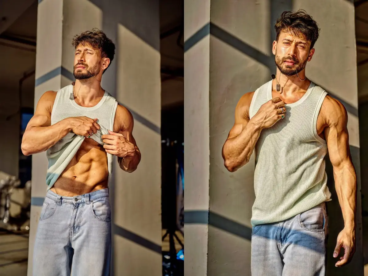
Lawrence Bishnoi gang claims responsibility for firing at Tiger Shroff over ties to Salman Khan
&imwidth=180&imheight=135&format=webp&quality=medium)
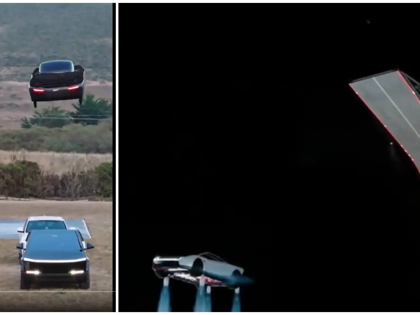
Flying car race: Alef Aeronautics welcomes Tesla Roadster '11 years' later, but are the two models the same?
&imwidth=180&imheight=135&format=webp&quality=medium)
Saudi Arabia asks skyscraper employees to work from home amid Houthi threats
&imwidth=180&imheight=135&format=webp&quality=medium)
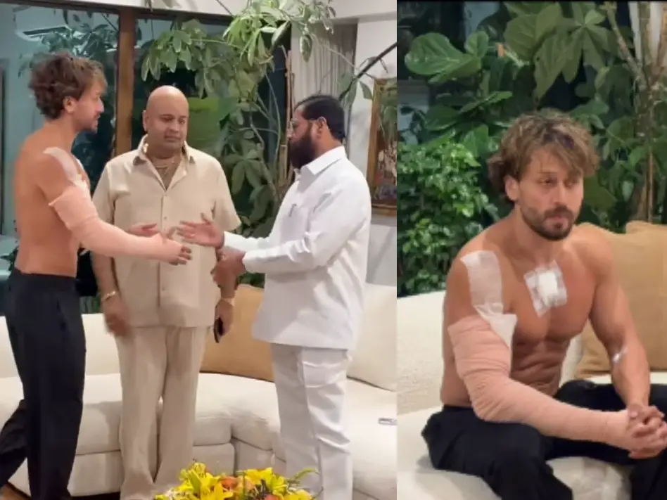
Tiger Shroff shows injuries after Juhu firing incident; Eknath Shinde says Mumbai won’t tolerate gang wars
&imwidth=180&imheight=135&format=webp&quality=medium)
NFl 2026/27 - Saints vs Steelers to go ahead in Paris next week despite protest
&imwidth=180&imheight=135&format=webp&quality=medium)
4 killed, 19 critically injured in grass fire at Canada's largest military base
&imwidth=180&imheight=135&format=webp&quality=medium)
Nobel laureate Machado, who dedicated prize to Trump, confirmed as Venezuela opposition leader
&imwidth=180&imheight=135&format=webp&quality=medium)
After Kennedy Center and reflecting pool disputes, Trump turns to Washington golf course plan amid legal battle
&imwidth=180&imheight=135&format=webp&quality=medium)
Why France looks the most fragile in the G7 amid protests and budget deadlock
&imwidth=180&imheight=135&format=webp&quality=medium)
China responds to Trump's Press Secretary Katie Zacharia after toilet remark: 'Visit China more often'
&imwidth=180&imheight=135&format=webp&quality=medium)
Cattle feed found in biscuits of Indian company, FSSAI sends legal notice
&imwidth=180&imheight=135&format=webp&quality=medium)
Anthropic’s public benefit plan: What its 5% share commitment means for AI’s future
&imwidth=180&imheight=135&format=webp&quality=medium)
Girl 'dead' for 8 hours wakes up at her own funeral, dad insists she wasn't breathing
&imwidth=180&imheight=135&format=webp&quality=medium)
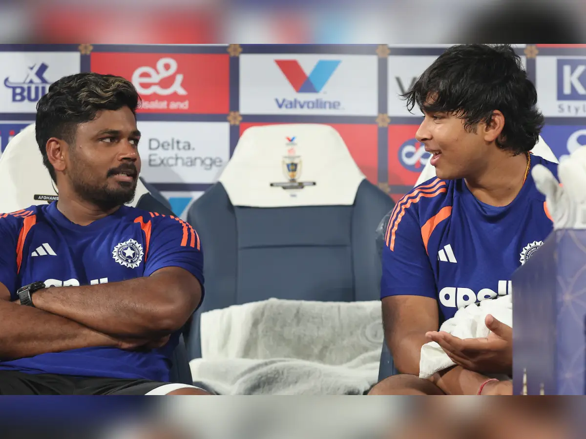
Pujara says 'Samson and Vaibhav cannot be in Playing XI' for India on NZ tour
&imwidth=180&imheight=135&format=webp&quality=medium)
MI5 is opening an AI threat centre, and OpenAI just told MPs the worst isn't over
&imwidth=180&imheight=135&format=webp&quality=medium)
WATCH | iPhones, luxury perfumes floating in Hormuz? Iranian fishermen make bizarre discovery
&imwidth=180&imheight=135&format=webp&quality=medium)
Elon Musk features on Lucknow's 'anti-India' Ravan poster alongside Rahul Gandhi, Akhilesh
&im=FitAndFill=(700,400)&imwidth=180&imheight=135&format=webp&quality=medium)
New OTT releases this week (October 19-25, 2026): Gajab Raat to Chaar Yaar-8 titles to watch during Dussehra week on Netflix, Prime Video and more
&imwidth=180&imheight=135&format=webp&quality=medium)
Kylie Jenner makes Victoria’s Secret debut in $50 million diamond-encrusted design as Timothée Chalamet cheers
&imwidth=180&imheight=135&format=webp&quality=medium)
Putin wants joint meeting with Trump-Xi summit on Ukraine war, proposes talks alongside APEC: Report
&imwidth=180&imheight=135&format=webp&quality=medium)
No Ravindra Jadeja, Yashasvi Jaiswal in India’s 2027 ODI World Cup plans: Report
&imwidth=180&imheight=135&format=webp&quality=medium)
India moves to buy 10,000 more AI chips for a national compute pool open to startups
&imwidth=180&imheight=135&format=webp&quality=medium)
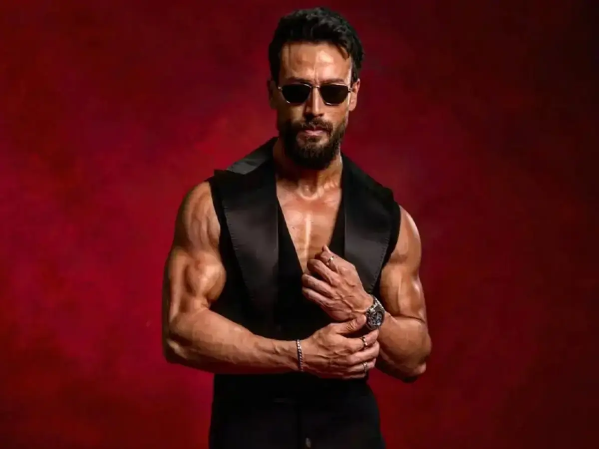
Tiger Shroff attacked by three gunmen in Mumbai, actor safe, two injured
&imwidth=180&imheight=135&format=webp&quality=medium)
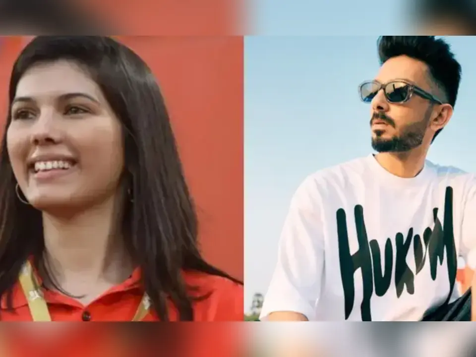
Anirudh Ravichander-Kavya Maran wedding: Telangana CM reveals Chennai reception date
&im=FitAndFill=(700,400)&imwidth=180&imheight=135&format=webp&quality=medium)
Tesla Roadster engineering: The hidden hardware behind its flying demonstration
&imwidth=180&imheight=135&format=webp&quality=medium)
US to review Russia sanctions waiver within 60 days as Rubio cites India’s ‘substantial’ Russian energy imports
&imwidth=180&imheight=135&format=webp&quality=medium)
'We feel like Mr India': Gujarat’s undercover SHE team guard garba nights at Navratri
&imwidth=180&imheight=135&format=webp&quality=medium)
Cattle-feed bran in biscuits, detergent in milk: FSSAI acts against 3 companies
&im=FitAndFill=(700,400)&imwidth=180&imheight=135&format=webp&quality=medium)
5 technologies that could make the Tesla Roadster one of the most unusual cars ever built
&imwidth=180&imheight=135&format=webp&quality=medium)
'It's a joy to see the makers bring it on such a grand scale': SS Rajamouli on Ramayana
&imwidth=180&imheight=135&format=webp&quality=medium)
Priest dies after crucifix falls on his head during livestreamed Mass in Ecuador | VIDEO
"We have been collaborating extensively with semiconductor industries worldwide on advanced nanoelectronics technologies, including solutions to ESD reliability threats to advanced SoCs. We have carried out both fundamental and applied research on ESD protection devices, with a strong emphasis on creating practical solutions for the semiconductor industry in a range of technology nodes,” said Mayank, who heads the MSDLab, and will be leading this collaborative effort.
Samsung Semiconductor India Research, a subsidiary of Samsung Electronics, is the technology hub enabling innovative growth in both hardware development as well as software-powered solutions in semiconductor technologies.
WATCH WION LIVE HERE
