India's defence electronics ambitions get a boost as RRP opens advanced chip packaging facility | Defence Pulse

&imwidth=600&imheight=450&format=webp&quality=medium "India's defence electronics ambitions get a boost as RRP opens advanced chip packaging facility | Defence Pulse")
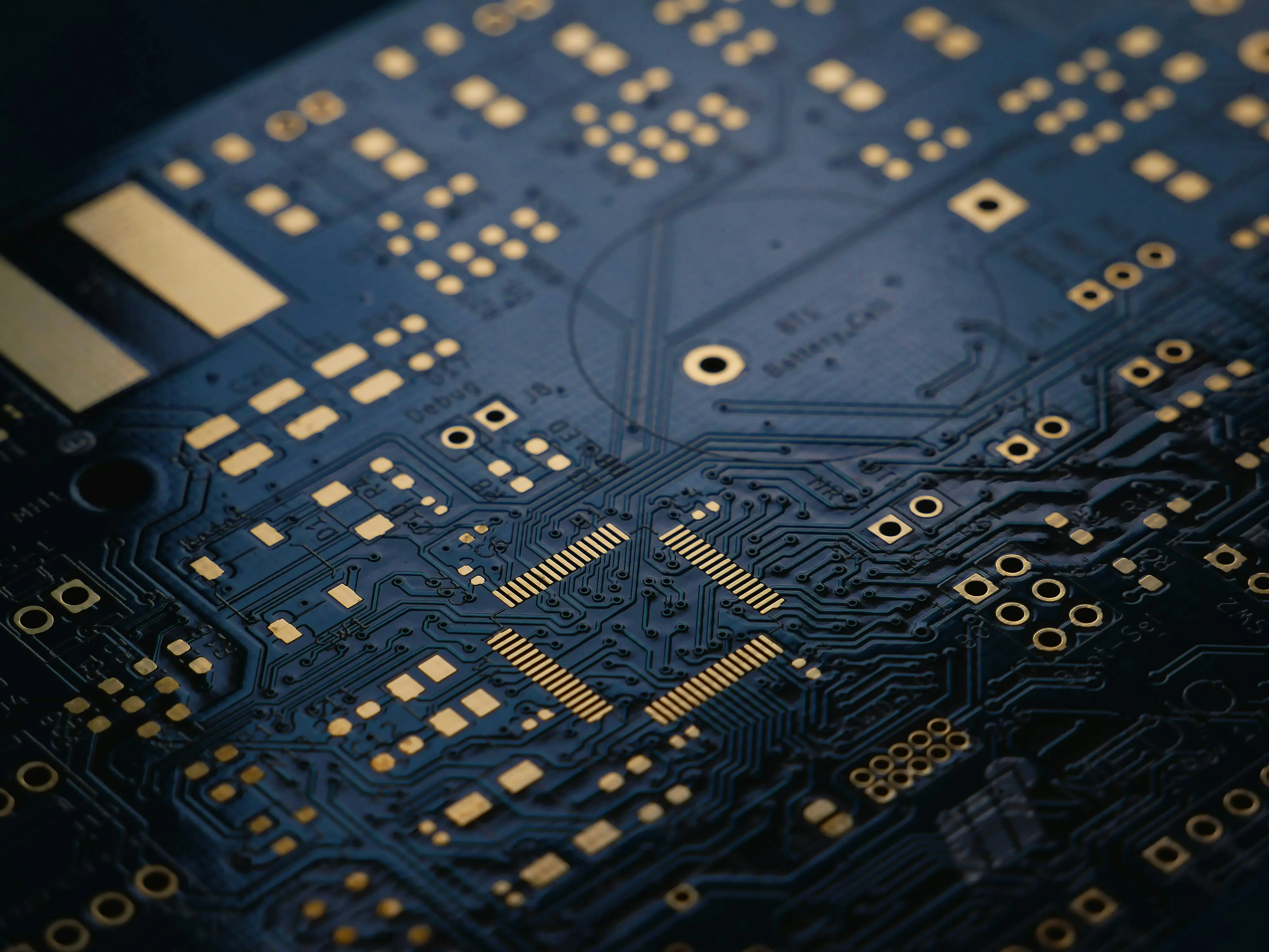
Representational Image Photograph: (Unsplash)
RRP Electronics has inaugurated an advanced wafer-level packaging facility in Maharashtra as India seeks to strengthen semiconductor self-reliance and reduce dependence on overseas suppliers for critical defence electronics.
India's push for semiconductor self-reliance has received a boost with RRP Electronics Limited inaugurating an advanced wafer-level packaging facility in Navi Mumbai, Maharashtra.
The development comes as semiconductors become increasingly critical to India's defence capabilities, powering everything from advanced radars and missile guidance systems to electronic warfare equipment, avionics and secure communications.
The facility expands RRP Electronics' semiconductor assembly and testing capabilities. According to the company, it will support advanced packaging, SIM and eSIM module manufacturing and specialised semiconductor applications.
Dr Satheesh Reddy Highlights India's Defence Electronics Needs
Former DRDO Chairman Dr G. Satheesh Reddy stressed the importance of building indigenous semiconductor manufacturing capabilities to strengthen India's defence ecosystem.
“One of the areas where we have been lacking is semiconductors, devices, components, detectors, sensors,” Reddy said.
Trending Stories
&imwidth=280&imheight=210&format=webp&quality=medium)
&imwidth=280&imheight=210&format=webp&quality=medium)
&imwidth=280&imheight=210&format=webp&quality=medium)
&imwidth=280&imheight=210&format=webp&quality=medium)
&imwidth=280&imheight=210&format=webp&quality=medium)
&imwidth=280&imheight=210&format=webp&quality=medium)
&imwidth=280&imheight=210&format=webp&quality=medium)
&imwidth=280&imheight=210&format=webp&quality=medium)
&imwidth=280&imheight=210&format=webp&quality=medium)
&im=FitAndFill=(700,400)&imwidth=280&imheight=210&format=webp&quality=medium)
&imwidth=280&imheight=210&format=webp&quality=medium)
&im=FitAndFill=(700,400)&imwidth=280&imheight=210&format=webp&quality=medium)
&imwidth=280&imheight=210&format=webp&quality=medium)
&imwidth=280&imheight=210&format=webp&quality=medium)
&imwidth=280&imheight=210&format=webp&quality=medium)
&imwidth=280&imheight=210&format=webp&quality=medium)
&imwidth=280&imheight=210&format=webp&quality=medium)
&imwidth=280&imheight=210&format=webp&quality=medium)
&im=FitAndFill=(700,400)&imwidth=280&imheight=210&format=webp&quality=medium)
&imwidth=280&imheight=210&format=webp&quality=medium)
&imwidth=280&imheight=210&format=webp&quality=medium)
&imwidth=280&imheight=210&format=webp&quality=medium)
&imwidth=280&imheight=210&format=webp&quality=medium)
&imwidth=280&imheight=210&format=webp&quality=medium)
&imwidth=280&imheight=210&format=webp&quality=medium)
&im=FitAndFill=(700,400)&imwidth=280&imheight=210&format=webp&quality=medium)
&imwidth=280&imheight=210&format=webp&quality=medium)
&imwidth=280&imheight=210&format=webp&quality=medium)
&imwidth=280&imheight=210&format=webp&quality=medium)
&imwidth=280&imheight=210&format=webp&quality=medium)
&imwidth=280&imheight=210&format=webp&quality=medium)
&imwidth=280&imheight=210&format=webp&quality=medium)
&imwidth=280&imheight=210&format=webp&quality=medium)
&imwidth=280&imheight=210&format=webp&quality=medium)
&imwidth=280&imheight=210&format=webp&quality=medium)
Highlighting their importance in military systems, he added, “Microelectronics has got important applications in the radars, electronic warfare system, avionics.”
Reddy emphasised that India must expand its semiconductor manufacturing and outsourced semiconductor assembly and testing facilities to reduce dependence on overseas suppliers.
“We need much more advanced facilities like what they have inaugurated today,” he said.
RRP Founder Identifies Three Major Challenges
Rajendra Chodankar, founder of RRP Electronics, identified three challenges that India must address to develop a competitive semiconductor manufacturing industry.
“First, obviously, skill set,” Chodankar said, stressing the need to involve academia, engineers, diploma holders and industrial training institute graduates in developing the workforce.
The second challenge, he explained, is the capital-intensive nature of semiconductor manufacturing, which makes government support and subsidies important.
“The most important thing is controlling rejections,” Chodankar said, highlighting the high rejection rates that manufacturers can face during initial production.
He warned that rejection rates could sometimes reach 80 per cent during the early stages, making process efficiency essential for commercial viability.
Building India's Semiconductor Supply Chain
Advanced wafer-level packaging involves creating electrical interconnections while integrated circuits remain part of a semiconductor wafer, before individual chips are separated.
The technology forms an important part of the manufacturing process, helping transform semiconductor designs into usable electronic components.
For RRP Electronics, the new facility represents another step towards expanding domestic capabilities in packaging, assembly, testing and module manufacturing.
For India's defence sector, the larger objective is to strengthen access to critical electronic components and develop a more resilient indigenous supply chain.
The challenge now lies in translating these investments into reliable, scalable semiconductor products capable of supporting India's growing civilian and military technology requirements.