

&imwidth=800&imheight=600&format=webp&quality=medium "Can India build complete semiconductor ecosystem beyond chip manufacturing? Experts weigh in")
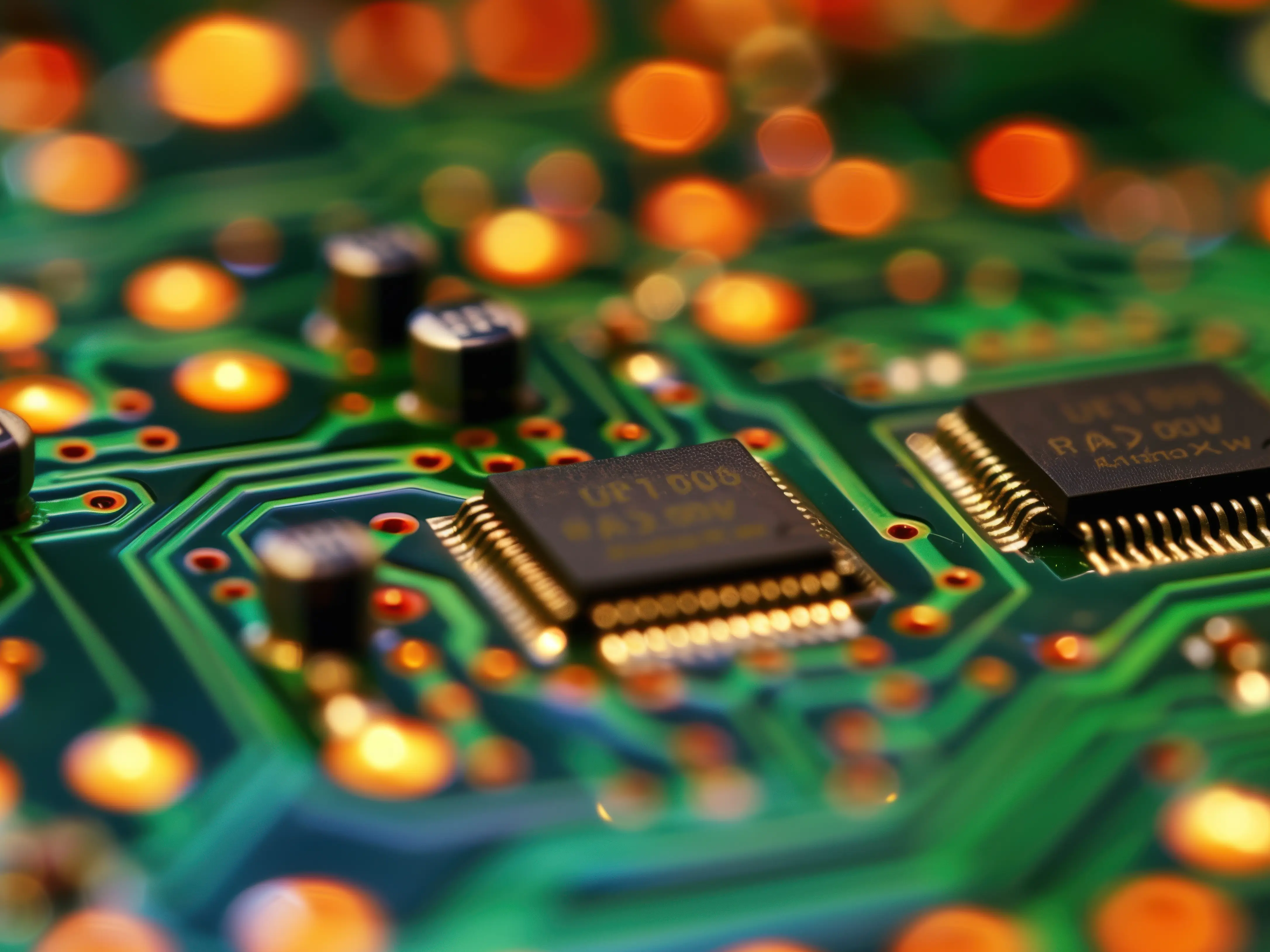
India’s plan for semiconductor ambitions has garnered significant momentum over the past few years. This comes with several government incentives, new fabrication units, and growing investor interest, putting the sector firmly in the national spotlight. In terms of design and intellectual property rights, India hosts nearly 20 per cent of the world's chip-design talent. Initiatives like the Design Linked Incentive (DLI) and Chips-to-Startup (C2S) programs aim to scale up to 200+ domestic chip-design startups and foster local system design.
Focusing on machines and materials, companies are also establishing manufacturing operations which can benefit from India's developing precision manufacturing ecosystem, which serves multiple sectors including aerospace, aviation, semiconductors and advanced electronics.
Another pillar of India’s semiconductor strategy focuses on diversifying fabrication across display, memory, silicon, compound and logic fabs, with growing global investor confidence. Advanced packaging is prioritised for its role in boosting system-level efficiency. R&D will be driven through industry-government-academia collaboration, with joint funding for applied projects aimed at tangible outcomes.
Talent development builds on roughly 400 universities currently offering chip-design education, with Semicon 2.0 upgrading curricula to help students advance from foundational chip design to systems design, strengthening India’s broader semiconductor capabilities.
Meanwhile, several industry experts warned that chip manufacturing alone will not be enough. Building a resilient, globally competitive semiconductor industry, they argue, requires India to develop capabilities across the entire value chain, from design and materials to packaging, testing, and end-use applications.
Beyond fabrication: The case for a full-stack ecosystem
Trending Stories
&imwidth=180&imheight=135&format=webp&quality=medium)
Sidhu Moose Wala’s younger brother wins hearts by recreating late singer’s signature move at Toronto Hologram Show
&imwidth=180&imheight=135&format=webp&quality=medium)
'I am thoroughly unamused': Judge slams Trump administration after 400 trees cut at Washington golf course
&imwidth=180&imheight=135&format=webp&quality=medium)
UK PM Andy Birnham renews claims of Russian meddling in Brexit vote
&imwidth=180&imheight=135&format=webp&quality=medium)
BCCI rejects venue shift reports, India vs Sri Lanka 1st ODI to remain in Delhi
&imwidth=180&imheight=135&format=webp&quality=medium)
Houthis warns US of 'painful response' if Washington joins Saudi war in Yemen as airlines suspend flights to Saudi Arabia
&im=FitAndFill=(700,400)&imwidth=180&imheight=135&format=webp&quality=medium)
New OTT releases this week (October 12-18, 2026): Sacrifice, Koffee with Karan S9, Roadies Rebirth- 6 titles coming on Netflix, JioHotstar and more
&imwidth=180&imheight=135&format=webp&quality=medium)
Elon Musk pumps $276 million into Republican campaigns ahead of US midterm elections
&im=FitAndFill=(700,400)&imwidth=180&imheight=135&format=webp&quality=medium)
Navratri 2026: 9 days, 9 forms of Goddess Durga and 9 colours- Check the complete list
&im=FitAndFill=(700,400)&imwidth=180&imheight=135&format=webp&quality=medium)
How does a robot decide what to do next?
&imwidth=180&imheight=135&format=webp&quality=medium)
Congress demands action against chief election commissioner
&imwidth=180&imheight=135&format=webp&quality=medium)
New Cold War: Why is China buying more gold? Explained
&imwidth=180&imheight=135&format=webp&quality=medium)
‘This is just the start’: Maaya Rajeshwaran on historic ITF title, confidence boost and future goals
&imwidth=180&imheight=135&format=webp&quality=medium)
Opposition’s 10 demands in Supreme Court petition range from stay on SIR to audit of voter rolls
&imwidth=180&imheight=135&format=webp&quality=medium)
1,500 drones illuminate Mumbai sky as Cordelia Cruises unveils second ship, Cordelia Sky
&imwidth=180&imheight=135&format=webp&quality=medium)
China’s gold rush puts billion in focus
&imwidth=180&imheight=135&format=webp&quality=medium)
Trump says he 'may' meet North Korean leader Kim Jong Un during upcoming Asia trip
&imwidth=180&imheight=135&format=webp&quality=medium)
'I will not be silenced': Ilhan Omar alleges political intimidation after federal officers search her Washington home
&imwidth=180&imheight=135&format=webp&quality=medium)
Pakistan's government blames PTI for rise of terrorism in Khyber Pakhtunkhwa
&imwidth=180&imheight=135&format=webp&quality=medium)
I.N.D.I.A. Bloc lists 10 requests to Supreme Court
&imwidth=180&imheight=135&format=webp&quality=medium)
'Ouch!!! That must hurt': Kangana Ranaut hails Kamal Haasan's sharp reply to Elon Musk over Starlink row
&imwidth=180&imheight=135&format=webp&quality=medium)
Anti-SIR protest in Mumbai: Protestors wear black masks & ribbons in Mumbai
&imwidth=180&imheight=135&format=webp&quality=medium)
‘Fortress breached, reclaimed’: CJP leaders enter Jantar Mantar a day after loss of protest venue status | WATCH
&imwidth=180&imheight=135&format=webp&quality=medium)
UK school ditches technology, shifts from screen to pen and paper for learning
&imwidth=180&imheight=135&format=webp&quality=medium)
Girl 'dead' for 8 hours wakes up at her own funeral, dad insists she wasn't breathing
&imwidth=180&imheight=135&format=webp&quality=medium)
Korean peninsula tensions escalate as North Korea launches multiple ballistic missiles, PACOM says 'no threat to US personnel'
&imwidth=180&imheight=135&format=webp&quality=medium)
Delhi protest: CJI Surya Kant declines to meet India Bloc leaders
&imwidth=180&imheight=135&format=webp&quality=medium)
Rahul Gandhi's plea against Election Commission delayed as Supreme Court registry flags 14 ‘defects’
&imwidth=180&imheight=135&format=webp&quality=medium)
Robotic surgery, advanced treatment: What is coming to this small Gujarat town?
&imwidth=180&imheight=135&format=webp&quality=medium)
Trump weighs firing Kimberly Guilfoyle as US ambassador to Greece amid misconduct allegations: Report
&imwidth=180&imheight=135&format=webp&quality=medium)
India's Ajit Doval, Iran's Mohsen Rezaei hold talks amid escalating West Asia tensions, discuss 'issues of mutual interest'
&imwidth=180&imheight=135&format=webp&quality=medium)
'Almost certainly': UK Prime Minister Andy Burnham says Iran's IRGC behind RAF Fairford threat
&imwidth=180&imheight=135&format=webp&quality=medium)
'Turn approver, resign, we'll forgive you': Rahul Gandhi claims receiving messages from CEC Gyanesh Kumar
&imwidth=180&imheight=135&format=webp&quality=medium)
'Absolutely disgusting': Australia slams US plan to livestream Nidal Hasan's execution; Mike Johnson raises concerns, warns of terrorist propaganda
Kajal Shah, Co-founder & CEO of Dreamfly Innovations, said that India’s semiconductor journey needs to extend well past the fabrication plant. "India’s semiconductor journey must go beyond chip manufacturing to include indigenous design, materials, packaging, testing, power electronics, and embedded systems. These capabilities are essential for building advanced applications in drones, aviation, aerospace, and electric mobility. At Dreamfly Innovations, we believe that collaboration between semiconductor, battery, electronics, and aerospace companies can help India create a resilient and globally competitive deep-tech ecosystem," Shah said.
Amarjeet Singh Tak, Head - Research and Microscopy Solutions at ZEISS India and Neighbouring Markets, echoed this view, arguing that India’s semiconductor vision should span “the entire value chain, including chip design, advanced manufacturing, equipment, materials, packaging, testing, software, research and end-use applications.”
"Building a resilient and globally competitive ecosystem will require coordinated development across these interconnected capabilities. The rapid advancement of artificial intelligence demonstrates the importance of collaboration. Progress in AI is being driven collectively by semiconductor manufacturers, cloud-service providers, research institutions, start-ups, universities and industry. No single organisation can address the complexity of this transformation independently. Sustainable innovation depends on ecosystems in which talent, infrastructure, research and commercial expertise work together. At ZEISS, more than 180 years of scientific and technological experience have taken us from optics and precision engineering to medical technology, semiconductor manufacturing and industrial quality solutions. This journey has reinforced our belief that enduring technological leadership is built through sustained investment in research, strong partnerships, skilled talent and the ability to anticipate changing needs. For India, the AI era presents an opportunity not only to adopt advanced technologies, but also to develop them. Priorities should include strengthening research infrastructure, supporting deep-tech enterprises, expanding semiconductor capabilities, fostering industry–academia collaboration and developing future-ready talent. The countries that lead in AI will be those that create strong foundations for discovery, enable breakthrough research and empower the next generation of scientists, engineers and entrepreneurs to contribute to global technological progress," Singh added.
Early days, but real momentum
Anil Joshi, Managing Partner, Unicorn India Ventures, said, "India is still at an early stage of building a complete semiconductor ecosystem, but the progress over the last few years has been significant. We have built strong capabilities in chip design and are seeing encouraging momentum in fabless companies and home-grown SoCs, while semiconductor fabrication and allied infrastructure are now beginning to take shape. The opportunity is to build the entire value chain—from design and IP to fabrication, packaging, testing, equipment and materials. This will require substantial capital, deep technical expertise and, most importantly, patience. India has the talent, engineering capability and market opportunity to make this happen."
Comparing the initiative with China, the Beijing factor looms large over this ambition. Under Semiconductor Mission 2.0, India has committed Rs 1,27,500 crore, dwarfed by China’s roughly $48 billion in state semiconductor support. China dominates the global assembly, testing and packaging (ATP) segment with a 30 per cent share and accounted for 42 per cent of global semiconductor equipment spending in 2024. China already controls a large share of global mature-node capacity and could soon approach half of worldwide output in that segment, the very space India’s new fabs are targeting.
Therefore, India’s future foundry and ATP units will focus mainly on legacy chips sized between 28nm and 110nm, while India’s engineers make up about a fifth of the global chip design workforce, a genuine edge, though rising competition from China for design talent could erode it.