

&imwidth=800&imheight=600&format=webp&quality=medium "Why India should have its own Manhattan Project as China makes EUV breakthrough in AI chipmaking")
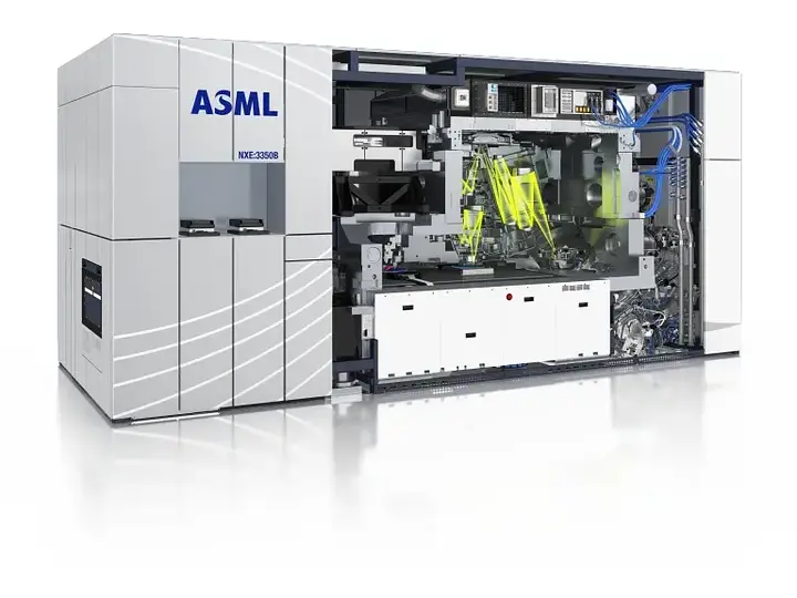
China's breakthrough in Extreme Ultraviolet (EUV) lithography for semiconductor manufacturing from its so-called 'Manhattan Project' is a leap forward in the nation's race towards self-reliance in artificial intelligence hardware. It also offers important lessons for India. Recent reports suggest that China built a ‘working prototype’ for indigenous EUV lithography. This is the world's first serious challenge to Dutch company ASML's monopoly in manufacturing EUV lithography machines. It is time to understand EUV lithography and why countries like India should launch their own mission-mode projects to achieve self-sufficiency in AI chipmaking.
What is EUV lithography machine and why is there a race to build them?
EUV lithography is the key technology that enables making the world's most advanced semiconductor chips. EUV lithography uses extreme ultraviolet light with a wavelength of 13.5 nanometres (nm) to print microscopic circuits on silicon wafers. This enables the manufacture of 5 nm, 3 nm and even smaller chips used for AI computing. These chips power smartphones, advanced computing systems, defence equipment and data centres. Smaller transistors improve computing speed, energy efficiency and processing power.
EUV manufacturing is extraordinarily complex. It requires extremely high precision, ultra-sophisticated optics, powerful light sources and consistently high production yields.
The Chinese project, often compared to the US Manhattan Project that developed the world's first nuclear weapons during the Second World War, brings together Huawei, state-backed research institutes and engineers who previously worked with ASML, the world's only commercial supplier of EUV lithography machines. Each of these machines costs approximately US$250-400 million.
The Chinese researchers, working in a high-security laboratory in Shenzhen are targeting the production of functional chips using EUV technology by 2028. Commercial production might realistically start in 2030.
Trending Stories
&imwidth=180&imheight=135&format=webp&quality=medium)
'It's a joy to see the makers bring it on such a grand scale': SS Rajamouli on Ramayana
&imwidth=180&imheight=135&format=webp&quality=medium)
Brendan Taylor overtakes Andy Flower to become Zimbabwe’s leading ODI run-scorer
&imwidth=180&imheight=135&format=webp&quality=medium)
Two Indians among 28 arrested in California over alleged voter registration fraud, DOJ says
&imwidth=180&imheight=135&format=webp&quality=medium)
Ramayana advance booking: Ranbir Kapoor, Yash's film cross $500K ahead of Diwali release
&imwidth=180&imheight=135&format=webp&quality=medium)
PCB omits Atherton, Hussain from tri-series commentary panel over Imran Khan interview row
&imwidth=180&imheight=135&format=webp&quality=medium)
Priest dies after crucifix falls on his head during livestreamed Mass in Ecuador | VIDEO
&imwidth=180&imheight=135&format=webp&quality=medium)
US Congressman Raja Krishnamoorthi describes foiled temple attack as ‘divine intervention’, criticises Vance and MAGA rhetoric
&imwidth=180&imheight=135&format=webp&quality=medium)
Pakistan betrays Iran, shuts border, trade as Trump moves towards new war
&imwidth=180&imheight=135&format=webp&quality=medium)
WATCH | Albania protesters set Supreme Court on fire as anti-Rama riots escalate
&imwidth=180&imheight=135&format=webp&quality=medium)
'Paris is going to be a Muslim city very soon': Trump blames immigration for France unrest, urges Macron to tighten border policies
&imwidth=180&imheight=135&format=webp&quality=medium)
Shastri backs Shami comeback; lauds Bhuvi and warns Bumrah on format workload ahead of World Cup
&imwidth=180&imheight=135&format=webp&quality=medium)
One dead after shooting near mosque in Columbus, Ohio. Here's what we know so far
&imwidth=180&imheight=135&format=webp&quality=medium)
Flying car race: Alef Aeronautics welcomes Tesla Roadster '11 years' later, but are the two models the same?
&imwidth=180&imheight=135&format=webp&quality=medium)
US Midterm 2026: What do opinion polls and prediction markets say less than two weeks before voting
&imwidth=180&imheight=135&format=webp&quality=medium)
Cattle-feed bran in biscuits, detergent in milk: FSSAI acts against 3 companies
&imwidth=180&imheight=135&format=webp&quality=medium)
Netanyahu rival Benny Gantz quits Israel election race, vows to push for unity government
&imwidth=180&imheight=135&format=webp&quality=medium)
'Whatever I can do to end this war': Trump floats China Summit with Putin and Xi, questions Zelensky's role in peace talks
&imwidth=180&imheight=135&format=webp&quality=medium)
India moves to buy 10,000 more AI chips for a national compute pool open to startups
&imwidth=180&imheight=135&format=webp&quality=medium)
Trump Commerce Secretary Howard Lutnick’s family fortune more than doubles to $7.3 billion, outpacing his boss
&imwidth=180&imheight=135&format=webp&quality=medium)
'We feel like Mr India': Gujarat’s undercover SHE team guard garba nights at Navratri
&imwidth=180&imheight=135&format=webp&quality=medium)
Girl 'dead' for 8 hours wakes up at her own funeral, dad insists she wasn't breathing
&imwidth=180&imheight=135&format=webp&quality=medium)
WATCH | Viral video shows woman jogging past burning barricade amid Paris unrest, sparks online debate
&imwidth=180&imheight=135&format=webp&quality=medium)
US midterm elections 2026: Early voting picks up pace ahead of November 3 polls
&im=FitAndFill=(700,400)&imwidth=180&imheight=135&format=webp&quality=medium)
New OTT releases this week (October 19-25, 2026): Gajab Raat to Chaar Yaar-8 titles to watch during Dussehra week on Netflix, Prime Video and more
&imwidth=180&imheight=135&format=webp&quality=medium)
France is burning. Trump blames immigrants. But who is answering Europe's real questions? | The Verdict
&imwidth=180&imheight=135&format=webp&quality=medium)
‘Spare India from anarchy’: Over 400 Indian-origin academics from MIT, Oxford condemn anti-CEC protests
&imwidth=180&imheight=135&format=webp&quality=medium)
Trump calls on New Mexico to become 'New America', claims 'home values and incomes would rise'
&imwidth=180&imheight=135&format=webp&quality=medium)
Baby orangutan rescued in India returns to Indonesia
&im=FitAndFill=(700,400)&imwidth=180&imheight=135&format=webp&quality=medium)
Ghaziabad is world's fastest-growing city; Surat, Patna, Rajkot also feature on list
&im=FitAndFill=(700,400)&imwidth=180&imheight=135&format=webp&quality=medium)
What is the real meaning behind Pete Hegseth's tattoos?
&imwidth=180&imheight=135&format=webp&quality=medium)
Pujara says 'Samson and Vaibhav cannot be in Playing XI' for India on NZ tour
&imwidth=180&imheight=135&format=webp&quality=medium)
WATCH | Japan launches historic mission to collect samples from Mars' moon Phobos
&imwidth=180&imheight=135&format=webp&quality=medium)
Pete Hegseth meets Benjamin Netanyahu during unannounced visit to Israel ahead of election
&imwidth=180&imheight=135&format=webp&quality=medium)
Kenyan cult leader found guilty over starvation deaths of nearly 200 children
China could commercialise EUV technology soon. What would it mean for the world?
Since 2019, US-led export restrictions prevented China from purchasing ASML's EUV systems, forcing it to develop indigenous alternatives. Once China develops the capability to manufacture chips using indigenous EUV lithography machines at scale, it could significantly reduce its dependence on foreign semiconductor equipment.
Domestic production of advanced chips would strengthen China's AI, electric vehicle, telecommunications and defence industries.
Increased chip production could also improve global supply and reduce costs over time.
A Chinese success in in commercialising EUV machines could make it eventually emerge as an exporter of advanced lithography equipment, creating competition in a market currently dominated by a single company, ASML.
US-China technology rivalry and China's EUV lithography breakthrough
ASML spent nearly two decades perfecting commercial EUV technology. China is now attempting to close that gap. If Beijing succeeds in commercialising indigenous EUV systems, it would weaken the effectiveness of US export controls that limited China's access to advanced semiconductor manufacturing. This could force the US and its allies to invest even more heavily in next-generation semiconductor manufacturing, while further intensifying the global technology race.
Why India should have its own Manhattan Project
This is where the India Semiconductor Mission (ISM) becomes important. India has approved projects worth over ₹1.6 trillion covering semiconductor fabrication plants, Outsourced Semiconductor Assembly and Test (OSAT) facilities, Assembly, Testing, Marking and Packaging (ATMP) units, and compound semiconductor projects. ISM 2.0 focuses on strengthening semiconductor equipment, materials, research, chip design and advanced packaging.
Yet, India still lacks leading-edge chip fabrication capability, a domestic semiconductor equipment ecosystem and sufficient high-end manufacturing expertise.
While India is globally recognised for its chip design talent, it continues to depend heavily on imports for advanced semiconductor manufacturing. This is why India needs its own "Manhattan Project" for semiconductors.
Such a project can succeed only through sustained government support, long-term investment and close collaboration between research institutions, universities and industry in AI hardware and semiconductor manufacturing.
Expanding research and development, strengthening semiconductor talent, attracting global technology partnerships, and building domestic capabilities in chip design, packaging, materials and manufacturing equipment should be national priorities.
Achieving Atmanirbhar Bharat, or self-reliance, will require greater private investment, policy stability and a realistic long-term strategy rather than relying solely on short-term subsidies.