'3nm technology': Why smaller chips are more powerful

Building 3-nanometre semiconductors allows manufacturers to pack 19 billion transistors onto a tiny chip. Reducing the distance electrical signals travel delivers a 15 per cent speed boost while consuming 35 per cent less battery power.

The 3-Nanometre Milestone
The global technology industry has rapidly transitioned to 3-nanometre (3nm) semiconductor manufacturing. However, ‘3nm’ does not describe the physical size of the chip itself; it represents the microscopic scale of the transistors, marking a massive engineering leap.
Packing Billions of Transistors
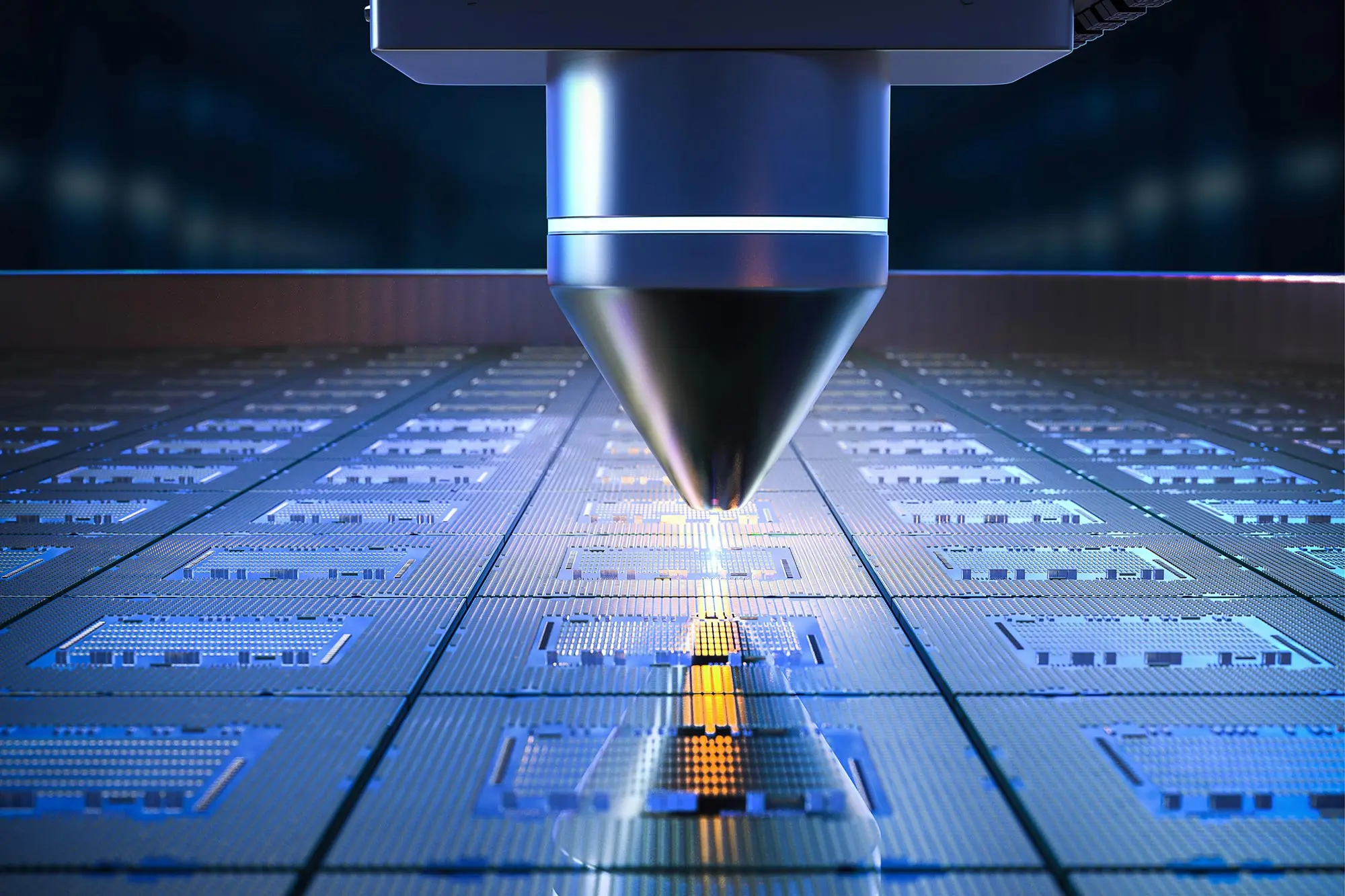
The smaller the manufacturing process, the more transistors engineers can cram onto a single piece of silicon. According to industry data, advanced 3nm smartphone processors now pack up to 19 billion transistors into an area smaller than a fingernail.
Faster Electrical Signals
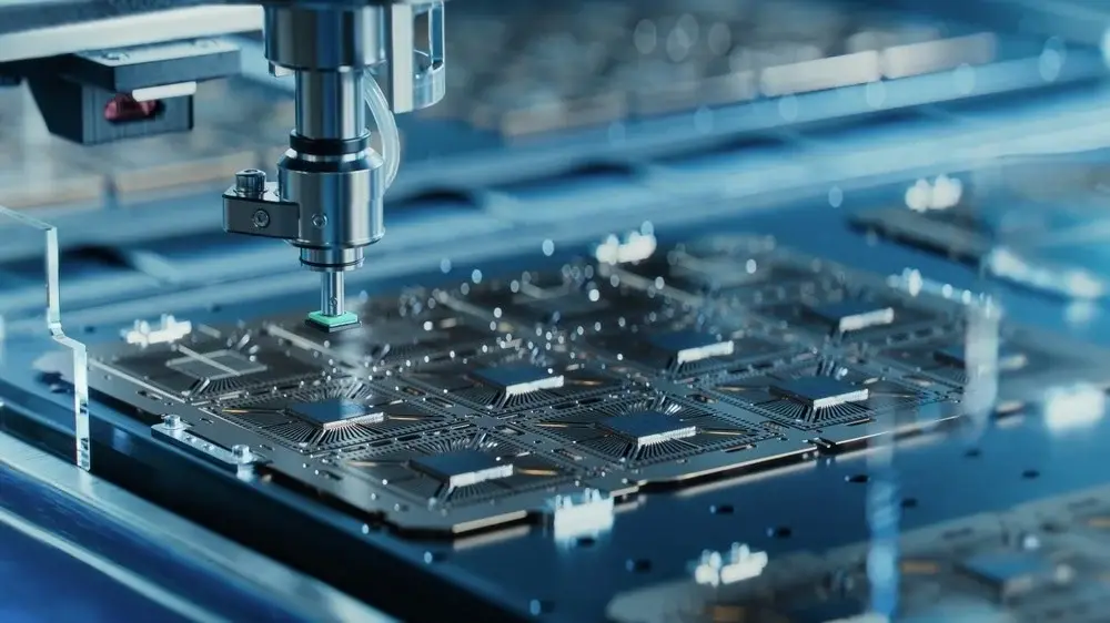
When microscopic transistors are placed closer together, internal electrical signals have a much shorter physical distance to travel. This proximity allows 3nm processors to communicate instantly, delivering a massive 15 per cent speed boost over previous 5-nanometre chips.

Massive Power Efficiency
Smaller transistors require significantly less voltage to switch on and off. Official metrics from TSMC show that a 3nm processor can execute the exact same heavy computational workload while consuming up to 35 per cent less power, drastically improving battery life.

Reduced Thermal Output
Because 3nm chips operate on lower voltages and utilise shorter electrical pathways, they lose far less energy as wasted heat. This superior thermal efficiency prevents flagship devices from overheating or throttling performance during intense artificial intelligence workloads.

Extreme Ultraviolet Manufacturing
Carving circuits at this microscopic scale is notoriously difficult. Tech giants use extreme ultraviolet (EUV) lithography machines to print these ultra-dense patterns, operating in strictly controlled cleanrooms to prevent dust from ruining the fragile silicon wafers.
The High Cost of Miniaturisation
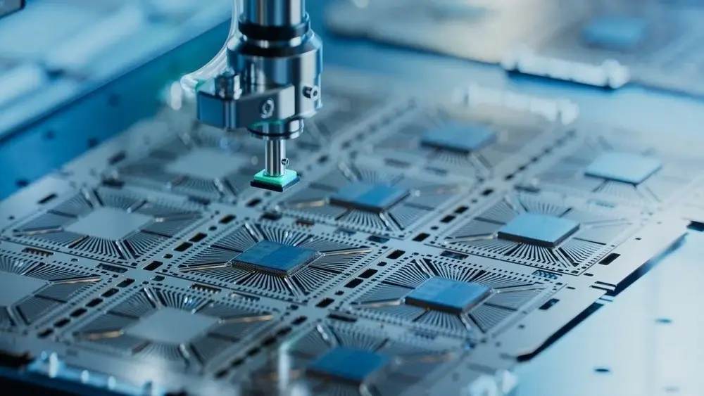
While 3nm technology offers unprecedented performance, it carries an astronomical financial burden. Producing a single 3nm silicon wafer costs approximately USD 20,000, forcing tech companies to heavily raise the retail prices of their premium smartphones and AI servers.
)
)
)
)
)